01 / Standard builds1
Standard builds
4L, 6L and 8L stack-ups
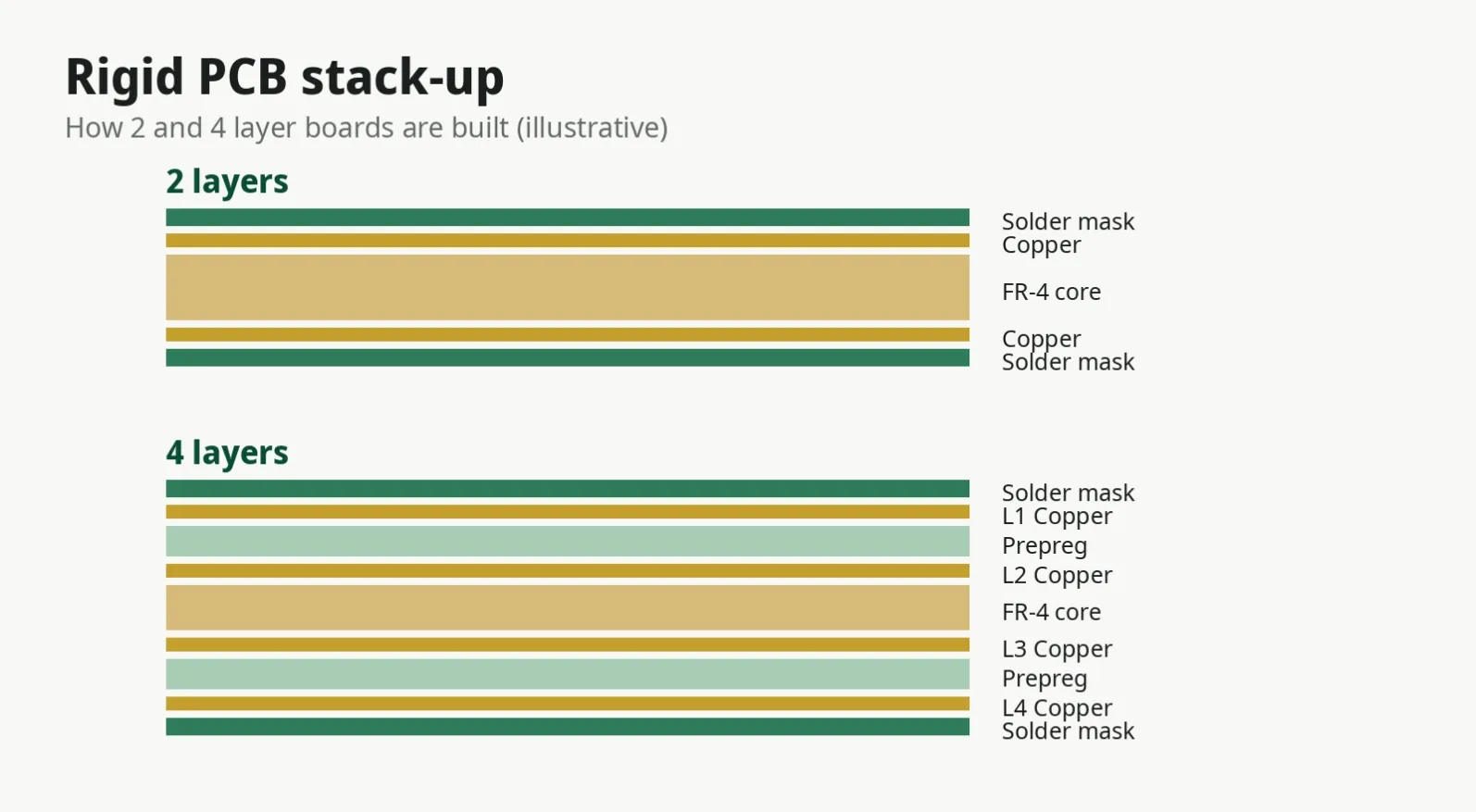
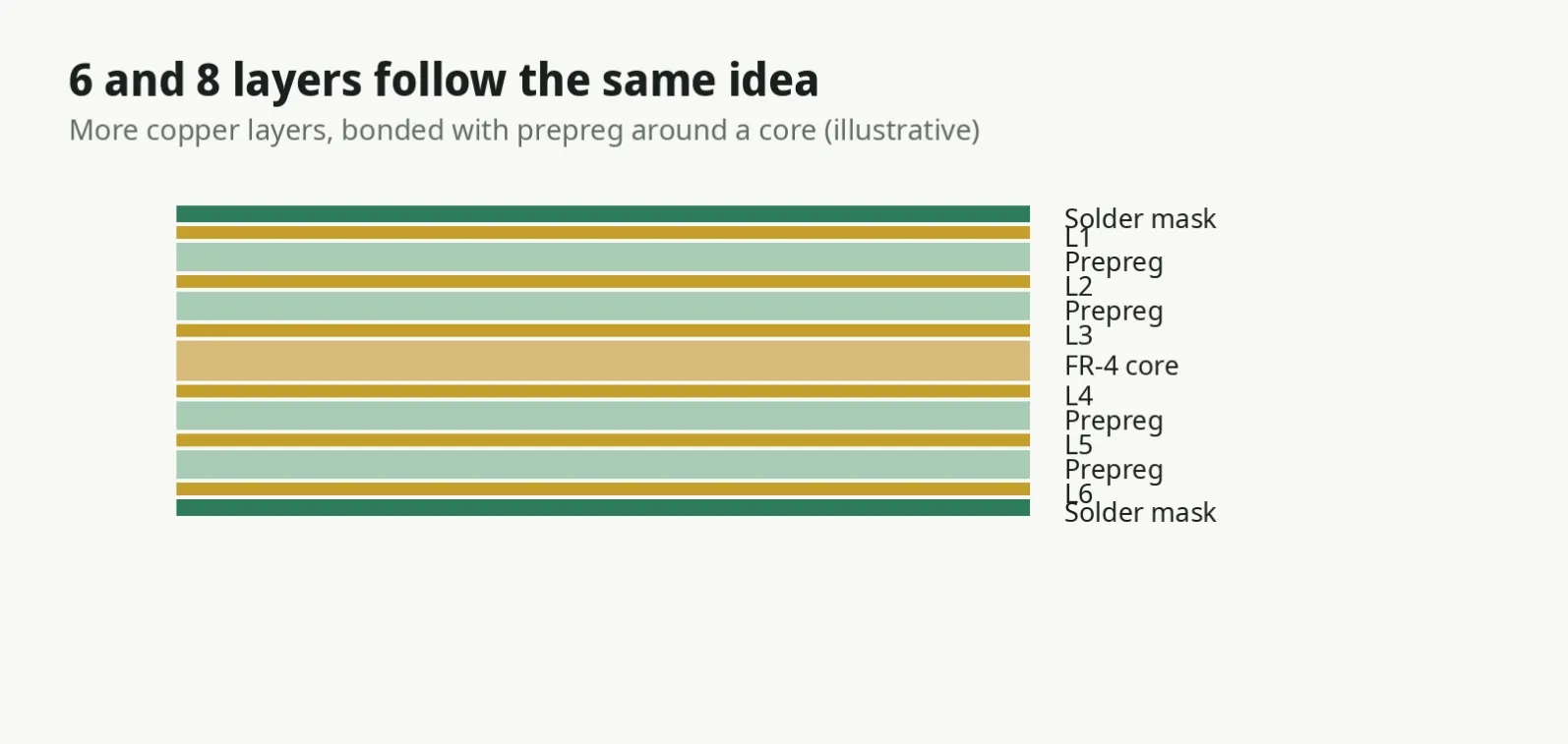
A stack-up is the sandwich your board is pressed from: copper layers separated by prepreg and core. It decides thickness, impedance behaviour and whether your board can be built at all.
4L, 6L and 8L stack-ups
0.4 to 3.2 mm
FR-4 (Shengyi, Kingboard)
Stack-up reviewed against your files
Cross-sections for each layer count
One core, copper on both sides. The prototype workhorse: cheap to iterate and fast to build.
Routing room plus dedicated power and ground planes. The most common step up when two layers stop working.
More signal layers for dense designs. Tell us the target finished thickness in your first message.
When you request a quote, give us the layer count and finished thickness. If your files imply a stack-up we cannot press, the review flags it before money moves.
Multilayer PCB fabrication from 4 to 8 layers: FR-4 stack-ups, 0.075 mm trace and space, ENIG, HASL and OSP finishes, prototype lead times from 5 to 7 working days.
FAQ
Still need help? Send us a note and we will point you in the right direction.
Email your Gerber and drill files to midst_zhong@126.com with layers, thickness, copper, finish and quantity — or start with the form and just the basics. Free engineer DFM check with every quote.